

Circuit Services Worldwide
Phone: (425) 454-7181
Fax: (425) 451-2956
10 148th Ave. NE
Suite 101
Bellevue, WA 98007
massey@csww-pcb.com
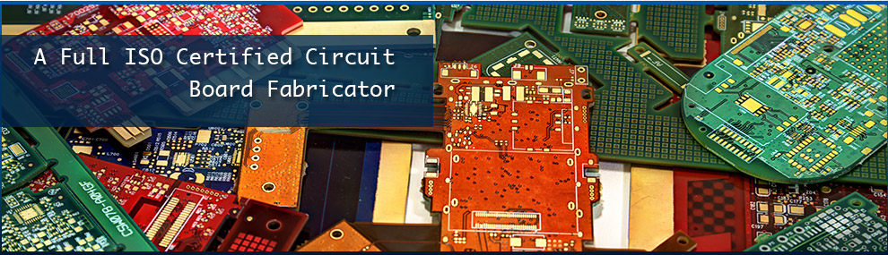
China Production - Manufacturing Capabilities
| Description | International Production |
| GENERAL | |
| Capacity (Avg. Daily) | S/S 30K SQFT, D/S 15K SQFT, MLB 25K SQFT |
| Current Utilization | 0.7 |
| Panel Sizes (inches) | 18*16, 18*24, 20*16, 21*24 |
| Layer Counts | 1 TO 36 LAYERS |
| Minimum DS lot size | 250 WORKING PANELS |
| Minimum 4 layer lot size | 200 WORKING |
| MATERIALS | |
| Laminates | FR-1, FR-2, CEM-1, -3 (above for single sided) & FR-4 *Tg 135 to Tg 175 degreeC) |
| Foils | COPPER FOIL |
| INNER LAYERS | |
| Foil Weight | 0.5 TO 4OZ |
| Minimum Line Width | 0.004" |
| Minimum Spacing | 0.004" |
| OVERALL BRD. THICKNESS | |
| Max. overall brd. thickness | 0.125" |
| Thickness tolerance | |
| Min. dielectric spacing | 0.003" |
| HOLES | |
| Min. drilled hole diam. | 0.007 |
| Max. drilled hole diam. | 0.25 |
| Plated hole tolerance | ��0.002" |
| Nonplated hole diam. Tolerance | ��0.002" |
| Hole/hole location accuracy | ��0.001" |
| Aspect ratio (finished) | 9:01 |
| Other\ Sequential Lamination process | |
| SOLDERMASK | |
| Type: | LPI MATTE/GLOSS |
| Application | AUTO SlLKSCREEN |
| Controlled thickness | YES |
| Registration tolerance | ��0.003" |
| Min. soldermask dam | 0.0023" |
| Available colors | GREEN ,RED,BLUE,BLACK |
| VIA PLUGGING | |
| Type | LPI THERMAL CURED |
| Max. hole size | 0.030" |
| Available colors | LPI THERMAL CURED |
| LEGEND | |
| Type | Silkscreen |
| Cure | UV |
| Available colors | WHITE,BLANK,YELLOW |
| Min. reproducible line | 0.006" |
| Location accuracy | 0.003" |
| Other | |
| SCORING | |
| Available angle | 30,45 DEGREE |
| Jump score | YES |
| ROUTING | |
| Edge to datum tolerance? | ��0.004" |
| Min. internal radius | RO 4mm |
| Rout tolerance | ��0.004" |
| Conductor to board edge | <0.007" rout< 0.020" screen? |
| EDGE BEVELING | |
| Available angles | 20 to 60 DEGRESS |
| Angle tolerance | ��5 DEGREE |
| Available depth | |
| Depth tolerance | ��0.004" |
| ELECTRICAL TEST | |
| Pitch | |
| Grid size | 0.012" |
| Fixtureless | FLYING PROBE TESTER |
| Test voltage | 150~250V |
| Net list capability | GERBER NET LIST CAD CAM NET LIST |
| FINISHES | |
| HASL | 40u" to 1000u" |
| Nickel/gold tab fingers | NI:50~200u" AU:5~20u" |
| Deep tank hard gold | 8" |
| ENIG (Electroless Ni /Immersion Au) | NI:50~200u" AU:5~20u" |
| OSP | YES |
| Silver in Hole | YES |
| Immersion Silver | YES |
| Immersion Tin | YES |
| Electrolytic Soft Gold | YES |
| Electroless Soft Gold | YES |
| Carbon Ink | YES |
| Eyelet pins | |
| Other | impedance control |
| LABORATORY | |
| Microsection | YES |
| Thermal stress | YES |
| Ionic contamination | YES |
| X-ray florescence | YES |
| Other | |
| Laser Direct Imaging | |
| Yag and CO2 Laser vias |